-Joseph Wilson
The following is an (lightly edited) excerpt from Joseph Wilson’s forthcoming book Humans of AI: Understanding the People Behind the Machines to be published by University of Toronto Press in Spring 2026. Copyright Joseph Wilson 2025. Reprinted with permission of the publisher.
“I picture the transistors as trembling bodies with translucent skin and fast, shallow breaths. They are utterly dependent on adults who cherish them for their extraordinary smallness and cosmic potential.” — Virginia Heffernan, Wired 2023
The Human Stack
If pundits in the media are to be believed, AI is on the cusp of transforming every aspect of human life: medicine, education, law, perhaps even rendering obsolete human labour. “Don’t get left behind!” CEOs are warned; “the future is here!” This kind of rhetoric positions AI as a force of nature, the next inevitable step jump in human progress. For this message to resonate, tech companies need to present their AI technologies as performing incredible feats of prediction, creation, and reasoning, completely unaided. But humans created every single piece of data that was used to create the AI models that made waves in 2023; they wrote the code that comprised the models; they nudged the models to make better decisions by telling them when they were right or wrong; they flagged offensive content that was in training data; and they designed the server farms and computer chips that ran the models. It’s not just the labour of a handful of people upon which the AI ‘tech stack’ has been built—it’s humans all the way down. It is this ‘human stack’ that gets ignored when we accept the myths spun by Silicon Valley.
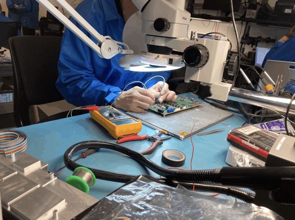
Figure 1: An engineer in the NextChipAI lab solders components to a circuit board.
By listening to the people who work on this technology we can move towards a deeper understanding of what AI is and what it’s capable of. Instead of treating AI as inevitable and all-powerful, we can step back and try to understand it as a product of a particular place, at a particular time, and made by a particular group of people. From 2023 to 2025 I conducted fieldwork as an intern at a company in Toronto I’ll call NextChipAI that designs specialized computer chips to run AI models. The regular silicon chips in your laptop can run any kind of program or application imaginable. They are versatile, but the tradeoff is that they’re relatively slow and use a lot of energy. In contrast, the chips designed by NextChipAI only do one thing: process neural networks. But they do so extremely quickly and efficiently. The engineers who design the layout of the circuits on these chips are at the bottom of the human stack and create a very real, physical foundation upon which the edifice of AI is built.
Making Sand Think
NextChipAI’s office is in a historic building in downtown Toronto; a standard 21st century open-concept workspace with rows of drop-in desks for software engineers, whiteboards on the walls, and nondescript meeting rooms. But on one side of the office, a small lab had been carved out, complete with screwdrivers, oscilloscopes, and soldering irons. While the manufacturing of the chips occurred off-site in Taiwan, the engineers in the lab were responsible for prototyping, testing, and designing the circuit boards that housed the chips. The hardware engineers were very proud of their position at the base of the stack. They sometimes typed code into computers, but mostly they engaged in visible tasks associated with making stuff: soldering, taking things apart, testing circuits, or connecting things with a bird’s nest of wires.
Shortly after I started at NextChipAI the employees celebrated a milestone they called “tape-out.” Designs for new chips are rendered in thousands of digital blueprints instructing the manufacturer in Taiwan what they want them to look like. Tape-out refers to the moment when the blueprints are finalized and sent off. The name comes from the early days of chip design in Silicon Valley when blueprint files were loaded onto magnetic tape reels and physically shipped to the factory. A large brass bell beside the front door was rung by one of the managers to mark the occasion. Tape-out was one of the moments where the software and hardware teams were united in their vision and could pause to celebrate their success.
In the lull that followed tape-out, hardware engineer Naomi explained to me how the chips were being made on the other side of the world. Silicon chips start out as sand, she explained. Just outside the tiny town of Spruce Pine, North Carolina, is a deposit of what Vince Beiser from Wired magazine calls “the purest natural quartz—a species of pristine sand—ever found on Earth.” This is the sand that makes up silicon microchips. This sand (little grains of silicon dioxide) is treated and purified until it is pure silicon and then poured into a cylinder shape where it crystalizes into the form needed for chips. These cylinders are then sliced into circular wafers around 1 mm thick.
Naomi described the clean rooms in which NextChipAI’s chips were being manufactured. “Anybody who works in a clean room has to wear something called a bunny suit. No, it’s not a costume with bunny ears, it’s just fully covered suits, booties, masks, gloves, hoods,” she said, “and before you enter the clean room you have to take an air shower to blow any possible particle off you.” The wafers are placed into machines that cost $150 million each and circuits are burned into the surface with UV light according to the patterns on the blueprints. Robots hang from tracks to carry the wafers around the factory so human hands don’t sully the perfectly polished surfaces. “Even the shapes of the light bulbs are specified to prevent any possible particle from falling on a wafer,” she said.
The manufacturing facility Naomi described is the legendary Taiwan Semiconductor Manufacturing Company (TSMC). TSMC is built on what is locally known as the Sacred Mountain of Protection in Taiwan, a shrine to ‘innovation and democracy,’ just 100 miles from mainland China. While some international observers worry that China could invade Taiwan at any time, many point out that the global interconnectedness of TSMC’s production facilities would make it nearly impossible for China to take it over. TSMC uses diamond saws from Japan, sand sourced from Brazil and North Carolina, and the photolithography machines are all made by a company in the Netherlands.
From Tape-out to Bring-up
At this point our human stack fans out into a sprawling network, connecting tens of thousands of scientists and engineers across the globe specializing in everything from geology to molecular chemistry to sub-atomic physics. “I can’t think of a type of engineering that wouldn’t be involved in building something like that,” said Jackson, a firmware engineer at NextChipAI. “That chip, when you really think about it, thousands of people participated in making it,” said hardware engineer Zaid. “If you want to even include the people we buy the IP from like [external vendors], oh my god… that chip, you could say easily, probably 30, 40 thousand people participated in that, it’s not like the two hundred people you see over here.”
The next milestone, three or four months later, was known as “bring-up.” This refers to the moment when a box of prototype chips arrives at the office and is ‘brought up’ to the lab for testing. In the spring of 2024, thirty-six prototypes of the new chip, each one the size of a post-it note, showed up at the office. A courier arrived at the office around midnight, straight from a flight from Taiwan. Around thirty employees stood in a half-crescent around the lab bench to get a first glimpse of the chips. A hardware engineer carefully cut open the box and slide out two plastic trays. The chips lying in the trays were polished to a high sheen and had the NextChipAI logo embossed on the front. Everyone clapped. The chips were then carefully inspected for visible defects and tested for electrical shorts (four failed).
Software and firmware engineers then tried to access different sections of the chip, sending test signals into the maze of grid-like circuits to see how far they could get before an error showed up on the terminal. I asked one of the junior engineers who was sitting in the lab during bring-up whether she was involved in getting anything running on the chip. “Well… not really,” she demurred. Neel, a software engineer cut in, “Yes you have! This is a complete team effort. There’s no one single person you can point to and say, ‘that’s why it’s working’.” The emphasis on the collective was a strict ethos to be adhered to at NextChipAI, one that differed markedly from the ‘autonomous AI’ message emanating from Silicon Valley.
A few weeks later, the chips were stress-tested physically: the maximum voltage and current they could handle; how much heat was generated; how fast certain programs could run. I came to understand that engineers used all their senses to diagnose problems in the lab: sight, sound, touch, even smell. One of the managers, Hayatham, told me, “I looked over and I saw one of the hardware guys bring a board up to his nose and thought, ‘ah, he’s debugging’.” Experienced engineers can detect the subtle smells of different components burning. “If you smell it, then why is it smelling?” Kai tells me sometime later. “Our components are rated for really high temperatures, right? Why would something smell every time you turn [it] on?” He compares this to the way an ideal system should run. “You turn something on you hear nothing, you smell nothing, it’s cool to the touch. Everything is just… clean,” he says.
‘Hard to Fathom’
After a few weeks of testing, the chips were shipped out to early customers, snug in their sleek metal casings. The drama of the invention process remained behind in the lab as the boxes travelled the world to their new owners. The engineers at NextChipAI had made something real, a contribution to AI that worked, but their work remained invisible. The people I worked with valued their identity as solvers-of-problems and makers-of-things. They built up a strong sense of collegiality in their teams. They remained driven to solve the never-ending stream of puzzles that emerged from complex computational systems. It seems strange to think that, without this collaboration, without the in-jokes and the board-smelling, the entire modern economy would grind to a halt. But this is how all modern technology is made: slowly, incrementally, with humans working together on hard problems.
But these human stories are removed from the product that gets unpacked from the cardboard box at the other end. Instead, we find ourselves staring at the computer screen in awe at what “AI can do.” This results in, to use Jeff Bezos’ memorable phrase, “artificial artificial intelligence,” an illusion that fuels the belief that AI is capable of much more than it really is. The stakes of this rhetorical move are high. If we care about how AI models work (and for whom they work) and if we want to ensure their impact on society is, on balance, positive rather than negative, we need to know who these humans are that work on AI. “Sometimes I feel… a little frustrated or something,” Lou, a senior firmware engineer at NextChipAI, told me one day. “I guess, when people talk about how Steve Jobs brought us the smartphone, right? He’s one guy. He did some neat stuff, I guess. But the amount of people and time and effort… decades. The amount of time and effort and energy [that] goes into every piece of technology that is around is hard to fathom.”
——
Joseph Wilson is a Ph.D. candidate in Anthropology at the University of Toronto.
——